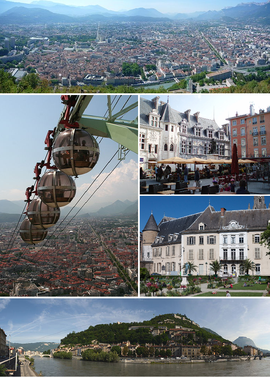
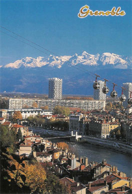
Grenoble -An attractive destination
Grenoble is the capital of the French Alpes, located in a valley surrounded by beautiful mountains. Stendhal once wrote that “… there is a mountain at the end of each Grenoble street: Belledonne, Vercors and Chartreuse…”. On the touristic side, Grenoble is famous for alpine landscapes, sunshine and snow.
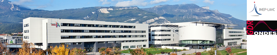
On the scientific side, Grenoble is often referred to as the place where the Silicon and SOI Valleys merge. Stendhal would certainly write today that “…there is research lab or high-tech place at the corner of each mountain."
A number of advanced R&D centres and leading semiconductor fabs are scattered around Grenoble. Application oriented research is blooming, its roots being the dense network of laboratories dedicated to basic research. World class institutes (European Synchrotron Radiation Facility, CEA, Neutron ILL reactor, etc) are surrounded by numerous smaller, yet outstanding University and CNRS laboratories.
Grenoble is one of the major university towns in France: over 60,000 students representing about 15% of the population of the greater Grenoble area. Grenoble is understandably proud of its academic and scientific environment, with a long tradition of partnership between research and industry.
Grenoble -Micro and Nanotechnology
Grenoble-Isère is the leading European centre for microelectronics on account of its integrated circuit technology and reseach. There are many examples illustrating the vitality and sophistication of the microelectronics activity in Grenoble area.
In 1992, STMicroelectronics, Léti-CEA and France Telecom R&D have pooled their deep sub-micronic technology research resources, with prototyping and production located at STMicroelectronics in Crolles.
In 2002, Freescale (Motorola) joined Philips and STMicroelectronics R&D alliance for 90- to 32-nm processes for 300-mm wafers in Crolles II. This is the largest industrial investment in France in the last 12 years.
A new 300 mm wafer fab has opened in 2003 at STMicroelectronics Crolles.
SOITEC is the world leader in the fabrication of SOI wafers (Smart-Cut process).
An active network of public research laboratories reporting to CNRS, INP Grenoble and UJF contributes to advanced projects and new concepts.
MINATEC has the ambition to become Europe's top centre for innovation and expertise in micro and nanotechnology. It is one of the few sites in the world to possess sufficient scientific, technological and industrial resources to achieve this objective. MINATEC will take form by developing cooperation networks and strategic alliances with complementary centres of excellence in France and elsewhere in the world. Minatec’s inauguration: June 1st 2006.
On 12 July, 2005, the Interministerial Committee for Regional Development (CIADT), chaired by the prime minister, approved the Minalogic project, granting it world-class competitivity centre status. This will enhance the international visibility of the Grenoble area and increase its drawing power.
The Minalogic competitivity centre aims to become the top centre in Europe, and one of the top three centres worldwide, for smart miniaturized solutions. It will bring together and consolidate resources from industry, research and training in two key fields: micro and nanotechnology, and systems-on-chip (SoC).